- 您现在的位置:买卖IC网 > Sheet目录3880 > PIC16F767T-I/ML (Microchip Technology)IC PIC MCU FLASH 8KX14 28QFN
PIC16F7X7
DS30498C-page 10
2004 Microchip Technology Inc.
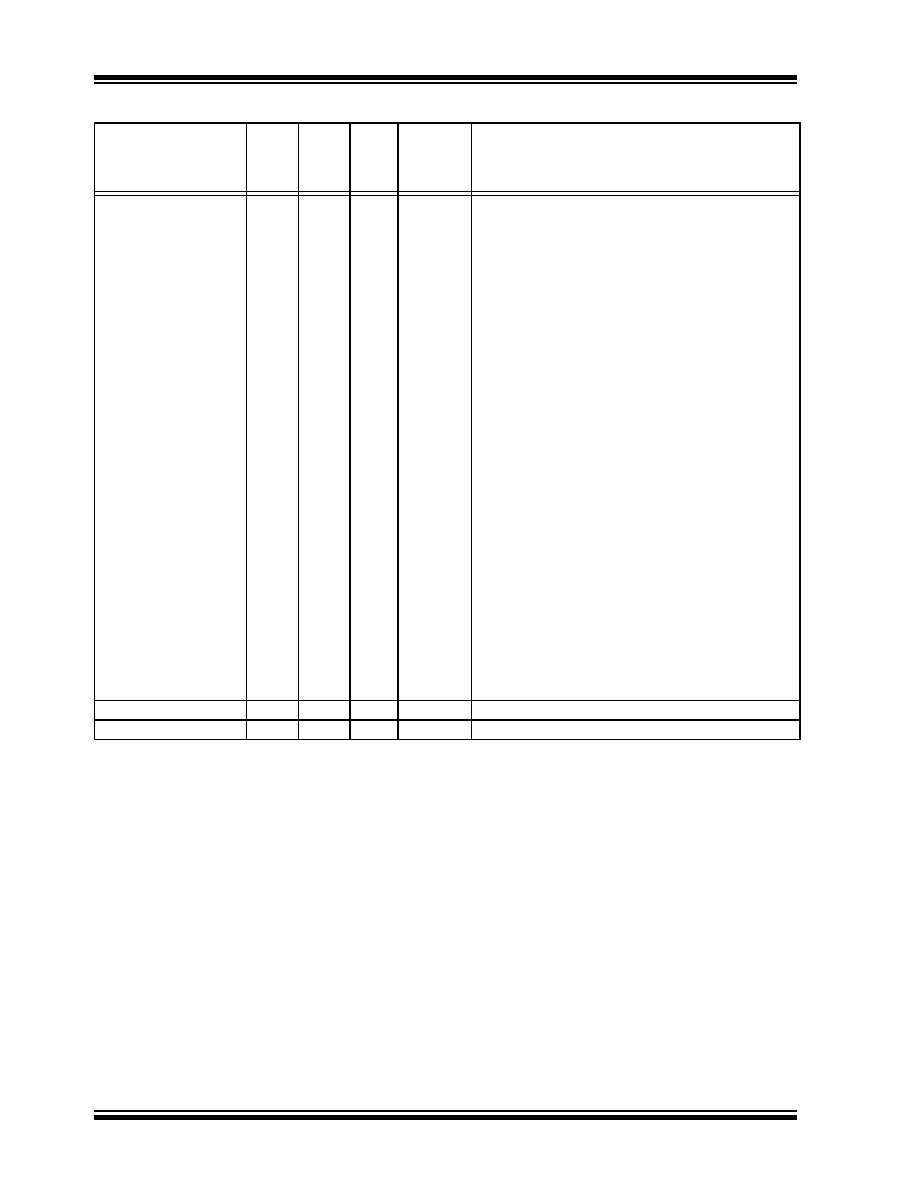
PORTC is a bidirectional I/O port.
RC0/T1OSO/T1CKI
RC0
T1OSO
T1CKI
11
8
I/O
O
I
ST
Digital I/O.
Timer1 oscillator output.
Timer1 external clock input.
RC1/T1OSI/CCP2
RC1
T1OSI
CCP2(4)
12
9
I/O
I
I/O
ST
Digital I/O.
Timer1 oscillator input.
Capture2 input, Compare2 output, PWM2 output.
RC2/CCP1
RC2
CCP1
13
10
I/O
ST
Digital I/O.
Capture1 input, Compare1 output, PWM1 output.
RC3/SCK/SCL
RC3
SCK
SCL
14
11
I/O
ST
Digital I/O.
Synchronous serial clock input/output for SPI mode.
Synchronous serial clock input/output for I2C mode.
RC4/SDI/SDA
RC4
SDI
SDA
15
12
I/O
I
I/O
ST
Digital I/O.
SPI data in.
I2C data I/O.
RC5/SDO
RC5
SDO
16
13
I/O
O
ST
Digital I/O.
SPI data out.
RC6/TX/CK
RC6
TX
CK
17
14
I/O
O
I/O
ST
Digital I/O.
AUSART asynchronous transmit.
AUSART synchronous clock.
RC7/RX/DT
RC7
RX
DT
18
15
I/O
I
I/O
ST
Digital I/O.
AUSART asynchronous receive.
AUSART synchronous data.
VSS
8, 19
5, 16
P
—
Ground reference for logic and I/O pins.
VDD
20
17
P
—
Positive supply for logic and I/O pins.
TABLE 1-2:
PIC16F737 AND PIC16F767 PINOUT DESCRIPTION (CONTINUED)
Pin Name
PDIP
SOIC
SSOP
Pin #
QFN
Pin #
I/O/P
Type
Buffer
Type
Description
Legend:
I = input
O = output
I/O = input/output
P = power
— = Not used
TTL = TTL input
ST = Schmitt Trigger input
Note
1:
This buffer is a Schmitt Trigger input when configured as the external interrupt.
2:
This buffer is a Schmitt Trigger input when used in Serial Programming mode.
3:
This buffer is a Schmitt Trigger input when configured in RC Oscillator mode and a CMOS input otherwise.
4:
Pin location of CCP2 is determined by the CCPMX bit in Configuration Word Register 1.
发布紧急采购,3分钟左右您将得到回复。
相关PDF资料
XF2L-1235-1
CONN FPC 12POS 0.5MM SMT
PIC16LF74-I/ML
IC MCU FLASH 4KX14 A/D 44QFN
PIC16F74-I/ML
IC MCU FLASH 4KX14 A/D 44QFN
PIC16LF819T-E/SS
IC PIC MCU FLASH 2KX14 20SSOP
XF2L-1025-1
CONN FPC 10POS 0.5MM SMT
PIC16LF737T-I/ML
IC PIC MCU FLASH 4KX14 28QFN
PIC16LF747T-I/ML
IC PIC MCU FLASH 4KX14 44QFN
XF2L-0835-1
CONN FPC 8POS 0.5MM SMT
相关代理商/技术参数
PIC16F767T-I/SO
功能描述:8位微控制器 -MCU 14KB 368 RAM 25 I/O RoHS:否 制造商:Silicon Labs 核心:8051 处理器系列:C8051F39x 数据总线宽度:8 bit 最大时钟频率:50 MHz 程序存储器大小:16 KB 数据 RAM 大小:1 KB 片上 ADC:Yes 工作电源电压:1.8 V to 3.6 V 工作温度范围:- 40 C to + 105 C 封装 / 箱体:QFN-20 安装风格:SMD/SMT
PIC16F767T-I/SS
功能描述:8位微控制器 -MCU 14KB 368 RAM 25 I/O RoHS:否 制造商:Silicon Labs 核心:8051 处理器系列:C8051F39x 数据总线宽度:8 bit 最大时钟频率:50 MHz 程序存储器大小:16 KB 数据 RAM 大小:1 KB 片上 ADC:Yes 工作电源电压:1.8 V to 3.6 V 工作温度范围:- 40 C to + 105 C 封装 / 箱体:QFN-20 安装风格:SMD/SMT
PIC16F76-E/ML
功能描述:8位微控制器 -MCU 14 KB 368 RAM 25I/O RoHS:否 制造商:Silicon Labs 核心:8051 处理器系列:C8051F39x 数据总线宽度:8 bit 最大时钟频率:50 MHz 程序存储器大小:16 KB 数据 RAM 大小:1 KB 片上 ADC:Yes 工作电源电压:1.8 V to 3.6 V 工作温度范围:- 40 C to + 105 C 封装 / 箱体:QFN-20 安装风格:SMD/SMT
PIC16F76-E/SO
功能描述:8位微控制器 -MCU 14KB 368 RAM 22 I/O RoHS:否 制造商:Silicon Labs 核心:8051 处理器系列:C8051F39x 数据总线宽度:8 bit 最大时钟频率:50 MHz 程序存储器大小:16 KB 数据 RAM 大小:1 KB 片上 ADC:Yes 工作电源电压:1.8 V to 3.6 V 工作温度范围:- 40 C to + 105 C 封装 / 箱体:QFN-20 安装风格:SMD/SMT
PIC16F76-E/SP
功能描述:8位微控制器 -MCU 14KB 368 RAM 22 I/O RoHS:否 制造商:Silicon Labs 核心:8051 处理器系列:C8051F39x 数据总线宽度:8 bit 最大时钟频率:50 MHz 程序存储器大小:16 KB 数据 RAM 大小:1 KB 片上 ADC:Yes 工作电源电压:1.8 V to 3.6 V 工作温度范围:- 40 C to + 105 C 封装 / 箱体:QFN-20 安装风格:SMD/SMT
PIC16F76-E/SS
功能描述:8位微控制器 -MCU 14KB 368 RAM 22 I/O RoHS:否 制造商:Silicon Labs 核心:8051 处理器系列:C8051F39x 数据总线宽度:8 bit 最大时钟频率:50 MHz 程序存储器大小:16 KB 数据 RAM 大小:1 KB 片上 ADC:Yes 工作电源电压:1.8 V to 3.6 V 工作温度范围:- 40 C to + 105 C 封装 / 箱体:QFN-20 安装风格:SMD/SMT
PIC16F76-I/ML
功能描述:8位微控制器 -MCU 14KB 368 RAM 22 I/O RoHS:否 制造商:Silicon Labs 核心:8051 处理器系列:C8051F39x 数据总线宽度:8 bit 最大时钟频率:50 MHz 程序存储器大小:16 KB 数据 RAM 大小:1 KB 片上 ADC:Yes 工作电源电压:1.8 V to 3.6 V 工作温度范围:- 40 C to + 105 C 封装 / 箱体:QFN-20 安装风格:SMD/SMT
PIC16F76-I/SO
功能描述:8位微控制器 -MCU 14KB 368 RAM 22 I/O RoHS:否 制造商:Silicon Labs 核心:8051 处理器系列:C8051F39x 数据总线宽度:8 bit 最大时钟频率:50 MHz 程序存储器大小:16 KB 数据 RAM 大小:1 KB 片上 ADC:Yes 工作电源电压:1.8 V to 3.6 V 工作温度范围:- 40 C to + 105 C 封装 / 箱体:QFN-20 安装风格:SMD/SMT